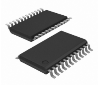


High-Speed ADC Chip - MS2510
Analog Input Range:
- Mode 1: 2V MAX
- Mode 2: 4V MAX
8-bit Resolution
Integral Linearity Error
±0.75 LSB(25℃) ±1 LSB(-20℃-75℃)
Differential Linearity Error
±0.5 LSB(25°C) ±0.75 LSB(-20℃-75℃)
Maximum Conversion Rate: 20MSPS
3.3V/5V Single Supply Operation
Low Power Consumption
Mode 1: 127.5mW
Mode 2: 150mW
Product Description
MS2510 is8bit,20MSPSADC (ADCs),using a half-flash architecture.MS2510operating at5Vsupply voltage, typical power consumption is only130mW, includes an internal sample-and-hold circuit, withhigh-impedance parallel output port and internal reference resistors.Compared to flash converters (flash converters), the half-flash architecture reduces power consumption and die size. By implementing conversion in a2step process (2-step process), the number of comparators is greatly reduced. Conversion data latency is2.5clock cycles.
I. Features of High-Speed ADC Chip MS2510:
Analog Input Range:
- Mode 1: 2V MAX
- Mode 2: 4V MAX
8-bit Resolution
Integral Linearity Error
±0.75 LSB(25℃) ±1 LSB(-20℃-75℃)
Differential Linearity Error
±0.5 LSB(25°C) ±0.75 LSB(-20℃-75℃)
Maximum Conversion Rate: 20MSPS
3.3V/5V Single Supply Operation
Low Power Consumption
Mode 1: 127.5mW
Mode 2: 150mW
II. Applications of High-Speed ADC Chip MS2510: